In our previous blog post, we discussed about Passive Optical Networks: what problems can the PONs target, which types are there and a bit of the state of the art. But a question was left unanswered: how can the Photonic Integrated Circuits boost these technologies? The PICs are known due to the exciting performance improvements when compared to traditional bulk technology: upgrades in terms of weight, volume, reduced power consumption, mechanical and thermal stability and assembly simplification for high subsystem integration are pointed as advantages[1].
The performance of PICs in PONs is recognized to allow high-speed transmission networks to support the faster interconnection between data centres[2]. It is even possible that an Optical Network Unit (ONU) and Optical Line Terminal (OLT) – see previous blog post – can coexist in the same PIC[1]).
What are Photonic Integrated Circuits?
PICs are electronic integrated circuits with optical components: modulators, detectors, attenuators, multiplexers, optical amplifiers and lasers[1]. PICs can be made of Indium Phosphide (InP) or Silicon Photonics (SiP)[3]. Each platform has its own characteristics and limitations and this directly implies in the PIC characteristics. For example, the InP platform allows the integration of both active (such as lasers) and passive elements (such as waveguides). Silicon Photonics takes advantage of the mature manufacturing developments in complementary metal–oxide–semiconductor (CMOS) and allows a high-volume and low cost PIC manufacturing[4]. Research is also developing to allow the use of integration platforms: simultaneously InP and SiP in the same PIC to combine active components on SiP platforms[4].
What do we need for data propagation?
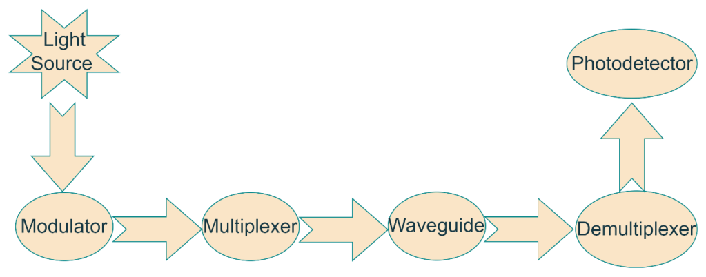
A source is used to generate continuous-wave light. The source can be off-chip or in-chip in case of InP or Heterogeneous platforms[5]. A modulator is used next to transfer data from the electrical to the optical domain. When more than one wavelength is needed, a multiplexer will combine the data in one wavelength to the waveguide. When outside the chip, the waveguide is usually the optical fibre, due to its several advantages over copper wires (see previous blog post). Then, a de-multiplexer will split the data back to the channels to a photodetector that will recover the data to the electrical domain[5]. Check out Figure 1 for the main building blocks of optical communication.
How can the light be coupled to the PICs?
The coupling should be the more efficient possible to increase the system performance. In the example of the silicon waveguides, this can have tens of nanometers and the core diameter of a single mode fibre (SMF), traditionally used in telecommunication systems, is near 10 microns. So, there is a mismatch between the fibre core and the waveguide from the chip, contributing to optical losses.
The coupling can be done by edge-coupling or using vertical grating couplers. In edge-coupling, the fibre-to-chip optical coupling is in-plane and vertical grating couplers use off-plane coupling[6].
Edge-coupling can achieve high coupling efficiencies, broad bandwidth, polarisation independence but has a footprint larger than the grating couplers, the coupling position is fixed[6] and, since the fibres need to be placed at the edges of the chip, this limits the number of inputs/outputs on the chip[5].
Vertical couplers are based on Bragg diffraction, which means that the fibres are placed on top of the gratings and the collection of light is possible if a resonance condition is seen: the waveguide propagation constant should match the horizontal component of the diffracted light. This is related to the effective refractive index of the waveguide and characteristics of the grating[5]. Grating couplers offer the flexibility of compact size, wafer level testing capability and flexible coupling position but also exhibit relatively low coupling efficiency (below 3 dB), narrow bandwidth and high wavelength sensitivity[6].
Both systems have advantages and drawbacks that should be taken into account when selecting the light coupling mechanism for each PIC.
But what is a grating?
A grating is a periodic arrangement of structures. Bragg gratings are formed by a series of submicrometer-scale periodic structures that obey to the Bragg condition, a resonance condition. Also, the reflected wavelength is named Bragg wavelength which is proportional to the effective refractive index and to the period of the index modulatio [7]. Its use can be in optical filters or reflectors and its applications can be optical networks, fibre lasers, fibre sensors and signal processors[8]. The Bragg gratings are being used in the telecommunications field since these are one of the most efficient modulation of the refractive index in the direction of propagation of mode. This modulation can be achieved intercalating to different materials or generating defects in the structure[9].
If you enjoyed this blog post, stay tuned to see the possibilities of light!
Blog Post Review
This blog post had the contribution of Professor António Teixeira to whom I would like to acknowledge.
